Midas – Hot Gas Rework System
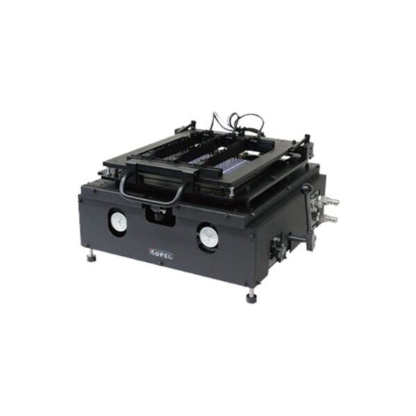
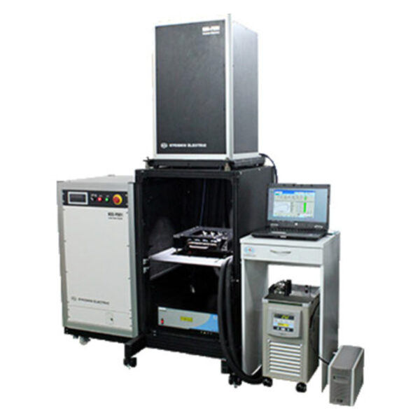
The HGRS-V is a highly adaptable dual-jet “thermal workbench” with a comprehensive suite of circuit-protective features. It’s the ideal solution for those facing a variety of rework tasks involving large die, eutectic attach, double-sided devices or other assemblies with tight thermal constraints.
Mitsubishi Materials – Low Alpha Tin/Silver (SnAg) bathes – SULA – for wafer plating with high plating rate
The SULA/UTB SnAg bathes are dedicated to semiconductor applications for wafer plating in order to produce bumps.
Mitsubishi Materials Corp. Electronics proposes a low-alpha product range particularly adapted to the semiconductor industry…
The SULA/UTB SnAg bathes are dedicated to semiconductor applications for wafer plating in order to produce bumps.
Mitsubishi Materials Corp. Electronics proposes a low-alpha product range particularly adapted to the semiconductor industry.
Mitsubishi Materials Corp. Electronics gets 95% of the global market share thanks to their products quality and their know-how. The flexibility and the reliability of their bathes offer a huge process window with the possibility to use current densities from 8 ASD to 15 ASD (up to 8µm/min).
NorCom – Optical Leak Test System – NorCom 2020
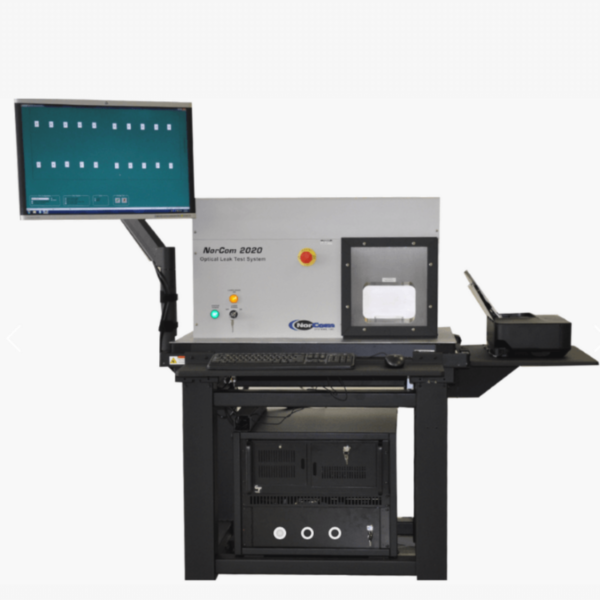
The NorCom 2020 provides automated in line, full matrix leak testing of hermetically sealed microelectronic and optoelectronic devices. It eliminates the need for helium mass spectroscopy and gross leak bubble testing by utilizi…
The NorCom 2020 provides automated in line, full matrix leak testing of hermetically sealed microelectronic and optoelectronic devices. It eliminates the need for helium mass spectroscopy and gross leak bubble testing by utilizing a patented laser interferometer to simultaneously measure gross and fine leaks in hermetic devices.
Since the reliability of hermetic electronic packages is dependent on the detection of gross and fine leaks, the NorCom 2020’s pinpoint accuracy, repeatability and increased production throughput make the system an essential requirement for hermetic device production.
Key Features
- High Throughput
- Automatic In-line Leak Detection
- Clean and Safe Procedure
Norcom 2020-WL
The NorCom 2020-WL inspects MEMS and other wafer level devices for both gross and fine leaks simultaneously while automatically rejecting all leaking devices. The system accepts up to an eight inch wafer that can be optionally loaded into the mach…
The NorCom 2020-WL inspects MEMS and other wafer level devices for both gross and fine leaks simultaneously while automatically rejecting all leaking devices. The system accepts up to an eight inch wafer that can be optionally loaded into the machine on saw frames measuring up to eleven inches square. The equipment is easy to setup and use, and the results can be networked to an SPC system for tracking all devices tested. It is ideal for leak testing any wafer level device that has an internal cavity. The system can inspect up to 1000 devices per cycle in both the singulated and un-singulated states.
Nordson EFD – HPx High-Pressure Dispensing Tool
HPx High-Pressure Dispensing Tool easily apply precise amounts of thick assembly fluids like epoxies and medical-grade adhesives through dispense tips as small as 0.004” with Nordson EFD HPx™ dispensing tools. Featuring a unique design, HPx to…
HPx High-Pressure Dispensing Tool easily apply precise amounts of thick assembly fluids like epoxies and medical-grade adhesives through dispense tips as small as 0.004” with Nordson EFD HPx™ dispensing tools. Featuring a unique design, HPx tools increase the pressure inside disposable syringe barrels up to seven times.
Nordson Electronics Solutions – Asymtek Forte® Series
Next-generation and time-tested capabilities are combined in this upgraded system to increase productivity by up to 50% over the top-selling Spectrum® ll, all in a space-saving footprint.
Nordson Electronics Solutions – Automated Plasma Treatment System – FlexTRAK® SHS
Industry-Leading Throughput and Reliability
Built upon Nordson Electronics Solutions’ patented plasma technology, the FlexTRAK®-SHS is our latest fully automated plasma system incorporating a high-capacity F3-S chamber, to provide …
Industry-Leading Throughput and Reliability
Built upon Nordson Electronics Solutions’ patented plasma technology, the FlexTRAK®-SHS is our latest fully automated plasma system incorporating a high-capacity F3-S chamber, to provide high uniformity and increased productivity. The chamber architecture remains the same as the smaller FlexTRAK platform, providing a seamless transition between chambers as production demands more capacity.
Key Applications
- Pre-wire bond plasma treatment on semiconductor package substrates and lead frames
- Pre-underfill plasma treatment on flip chip packages
- Pre-mold plasma treatment on semiconductor package substrates and lead frames
- Plasma treatment of semiconductor package substrates and lead frames for improved adhesion
- Removal/reduction of oxidation on lead frame
Nordson Electronics Solutions – Plasma Polymerization Deposition System – PD Series
Nordson Electronics Solutions introduces its PD Series Plasma Deposition Systems family, which uses plasma polymerization to deposit thin films uniformly during precision manufacturing and assembly processes to change the surfac…
Nordson Electronics Solutions introduces its PD Series Plasma Deposition Systems family, which uses plasma polymerization to deposit thin films uniformly during precision manufacturing and assembly processes to change the surface characteristics of a substrate. Plasma deposition can be used for applications in a wide range of industries, including medical, life sciences, industrial, semiconductor, MEMS, plastics, and electronics.
The PD Series for plasma deposition uses a gas vapor or heated liquid monomer vapor delivery system to deposit coatings that can reduce, and in certain cases eliminate, tackiness, provide a tie layer, make surfaces more slippery or resistant to corrosion, act as a drug enhancement or inhibition agent in life sciences applications, and change desired surfaces from hydrophobic to hydrophilic or vice versa. Polymers can be directly attached to a desired surface while the chains are growing, which reduces the steps necessary for other coating processes such as grafting. This is very useful for pinhole-free coatings of 100 picometers to 1 micrometer thickness with solvent insoluble polymers.
Key Features
-
Low-temperature processing because plasma energy is the catalyst for film growth.
- Plasma deposition is uniform and applies coatings evenly over curved or varied-level surfaces.
- Precise control of film thickness.
- Eliminates wet chemistry. Because polymers are deposited directly from the monomer, there are no waste streams due to wet chemical synthesis or solvents.
- Exhibits similar properties to those created via standard chemical polymerization techniques.
- Can be used in multiple steps during device manufacture: pre-treat the surface, deposit material, and apply functionalized polymer films.
Nordson Electronics Solutions – Plasma Systems – Sphere Series
SPHERE series systems support automated handling and processing of round or square wafer/substrate sizes ranging from 75mm to 300mm. In addition, thin wafer processing with or without carriers is possible, depending upon wafer t…
SPHERE series systems support automated handling and processing of round or square wafer/substrate sizes ranging from 75mm to 300mm. In addition, thin wafer processing with or without carriers is possible, depending upon wafer thickness.
The patented plasma chamber design provides exceptional etch uniformity and process repeatability. Primary plasma applications include a variety of etching, ashing, and descum steps. Other plasma processes include contamination removal, surface roughening, increasing wettability, and enhancing bonding and adhesion strength, photoresist/polymer stripping, dielectric etch, wafer bumping, organic contamination removal, and wafer destress.
- Wafer Cleaning – The SPHERE series plasma systems remove contamination prior to wafer bumping, remove organic contamination, remove fluorine and other halogen contamination, and remove metal and metal oxides. Plasma also improves spun-on film adhesion and cleans metallic bond pads.
- Wafer Etching – Plasma systems descum wafer of residual photoresist and BCB, pattern dielectric layers for redistribution, strip/etch photoresist, enhance adhesion of wafer applied materials, remove excess wafer applied mold /epoxy, enhance adhesion of gold solder bumps, destress wafer to reduce breakage, improve spun-on film adhesion, and clean aluminum bond pads.
Nordson Electronics Solutions – Vacuum Plasma Treatment Systems – AP Series
AP series plasma treatment machines are suitable for a wide variety of plasma cleaning, surface activation and adhesion improvement applications. These capabilities are used for semiconductor manufacturing, microelectronic packa…
AP series plasma treatment machines are suitable for a wide variety of plasma cleaning, surface activation and adhesion improvement applications. These capabilities are used for semiconductor manufacturing, microelectronic packaging and assembly, and by manufacturers of medical and life science devices. The AP Series consists of four batch plasma treatment systems offering small, mid-size and large vacuum chamber options that deliver process correlation, controller continuity and reliable, reproducible vacuum gas plasma treatment to customers as they expand from an R&D environment to various levels of production.
Nordson PBA – Melt Glue Applicator and Dispense Robot
Nordson’s MiniBlue II applicator provides the longest service life of any pneumatic gun in the packaging industry. MiniBlue II applicators apply adhesive at high speeds with dispensing times as low as 2 millisecond…
Nordson’s MiniBlue II applicator provides the longest service life of any pneumatic gun in the packaging industry. MiniBlue II applicators apply adhesive at high speeds with dispensing times as low as 2 milliseconds.
The Unity Basic Series systems are engineered for precise hot melt dispensing using Nordson Unity dispensing systems.
NTK Ceratec – Chuck repair service (6”, 8” and 12”)
The chuck repair service is dedicated to wafer chucks damaged in device manufacturing processes to a state equivalent to new using our vast knowledge of ceramics.
• for photolithography on ASML, Nikon, Canon, …
The chuck repair service is dedicated to wafer chucks damaged in device manufacturing processes to a state equivalent to new using our vast knowledge of ceramics.
• for photolithography on ASML, Nikon, Canon, …
• for Etching/CVD on Novellus (LAM), SPTS, Anelva, Nissim, …
Please, consult us for machine compatibilities and designs.
NTK Ceratec – Electrostatic Chuck
Electrostatic chucks and ceramic heaters can be produced by sintering materials with metallic electrodes arranged in the ceramics. We can provide electrostatic chucks and ceramic heaters catering to user needs by utilizing sever…
Electrostatic chucks and ceramic heaters can be produced by sintering materials with metallic electrodes arranged in the ceramics. We can provide electrostatic chucks and ceramic heaters catering to user needs by utilizing several material technologies. We can also provide services for the development and experimental production of electrostatic chucks and ceramic heaters according to region of use such as plasma and electron beam environments:
Electrostatic chuck with heater (ESC/Heater)
Material: AIN (Aluminum nitride)
Electrostatic chucks (ESC)
Material: Al2O3(Alumina) plate
Material: Thermal sprayed Al2O3
Ceramic heater
Material: AIN (Aluminum nitride)
NTK Ceratec – Porous Chuck
The original manufacturing method enhances adhesiveness between porous sections and base sections to achieve sufficient flatness even at boundary sections.
We can provide highly productive and reliable wafer thinning processing and manufact…
The original manufacturing method enhances adhesiveness between porous sections and base sections to achieve sufficient flatness even at boundary sections.
We can provide highly productive and reliable wafer thinning processing and manufacturing requiring whole surface absorption of large sized substrates.
We offer a wide selection of porous bodies with using different materials and pore sizes to cater to user needs.
NTK Ceratec – Vacuum Chuck
We can provide optimal pin chucks tailored to strict requirements through customized design using world-class flattening process technology (flatness of 0.2 μm for 12-inch chucks).
Can flexibly be adjusted planar shapes of pin chucks with …
We can provide optimal pin chucks tailored to strict requirements through customized design using world-class flattening process technology (flatness of 0.2 μm for 12-inch chucks).
Can flexibly be adjusted planar shapes of pin chucks with variable unevenness according to the shapes of wafers and customize absorption zones and pin patterns to enhance absorption responsiveness:
Nutek – Bare Board Loader With Pass Through Mode – Standard Series
Bare Board Loader With Pass Through Mode is used for loading of bare PCBs to the production line.
Nutek – High Speed Mini Loader
This unit is used for loading of substrates, leadframes or carriers.
Nutek – Laser Marking Cell Series – Standard Series
Nutek – Laser Marking Cell Series 3 unit is used to mark text, barcode, 2D code & graphic onto PCBs.
Nutek – Laser Marking Cell Series 5 unit is used to mark text, barcode, 2D code …
Nutek – Laser Marking Cell Series 3 unit is used to mark text, barcode, 2D code & graphic onto PCBs.
Nutek – Laser Marking Cell Series 5 unit is used to mark text, barcode, 2D code & graphic onto PCBs.
Nutek – PCB Inverter – Standard Series
This unit is used to invert PCBs (180°) for “double-sided” process.
Nutek – PCB Reject Conveyor – Standard Series
Faulty boards can be lifted up for visual inspection without interrupting the PCBs flow.
Nutek – Push Up Stacker – Standard Series
This unit is used for restacking of PCBs from the production line.
Nutek – Stack Leadframe/ Magazine Loader – Semicon Series
This unit is used for loading of substrates, leadframes or carriers.
Nutek – Telescopic Gate Conveyor (Normally Closed) – Standard Series
This unit is used when a passage way is required in a production line (fully automatic).
Nutek – Traverser & Shuttle Conveyor – Standard Series
This unit is used to redirect flow of PCBs into different channels in a production line.