NTK Ceratec – Chuck Repair Service (6”, 8” and 12”)
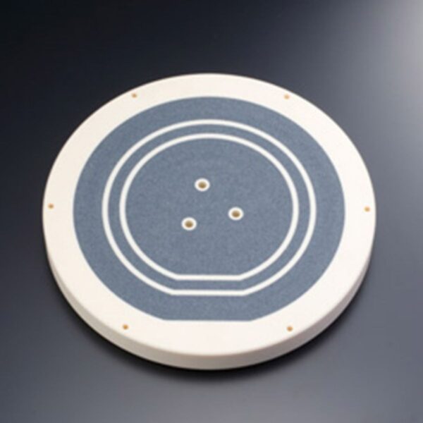
The chuck repair service is dedicated to wafer chucks damaged in device manufacturing processes to a state equivalent to new using our vast knowledge of ceramics.
The chuck repair service is dedicated to wafer chucks damaged in device manufacturing processes to a state equivalent to new using our vast knowledge of ceramics.