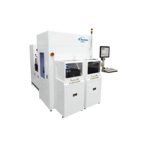
Nordson Electronics Solutions – Plasma Systems – Sphere Series
SPHERE series systems support automated handling and processing of round or square wafer/substrate sizes ranging from 75mm to 300mm. In addition, thin wafer processing with or without carriers is possible, depending upon wafer t…
SPHERE series systems support automated handling and processing of round or square wafer/substrate sizes ranging from 75mm to 300mm. In addition, thin wafer processing with or without carriers is possible, depending upon wafer thickness.
The patented plasma chamber design provides exceptional etch uniformity and process repeatability. Primary plasma applications include a variety of etching, ashing, and descum steps. Other plasma processes include contamination removal, surface roughening, increasing wettability, and enhancing bonding and adhesion strength, photoresist/polymer stripping, dielectric etch, wafer bumping, organic contamination removal, and wafer destress.
- Wafer Cleaning – The SPHERE series plasma systems remove contamination prior to wafer bumping, remove organic contamination, remove fluorine and other halogen contamination, and remove metal and metal oxides. Plasma also improves spun-on film adhesion and cleans metallic bond pads.
- Wafer Etching – Plasma systems descum wafer of residual photoresist and BCB, pattern dielectric layers for redistribution, strip/etch photoresist, enhance adhesion of wafer applied materials, remove excess wafer applied mold /epoxy, enhance adhesion of gold solder bumps, destress wafer to reduce breakage, improve spun-on film adhesion, and clean aluminum bond pads.