Showing 126–150 of 172 results

  • PBT Works – MiniSWASH

    This machine is a budget solution for anyone who does not expect to clean PCBAs on daily basis. Typically Research and Development centres, prototyping, start-ups and very low volume producers would find this machine sufficient ...

    This machine is a budget solution for anyone who does not expect to clean PCBAs on daily basis. Typically Research and Development centres, prototyping, start-ups and very low volume producers would find this machine sufficient to achieve great results.

    Application: Standard SMD Assemblies. Capacity: Small Volume Contamination Solubility: Easy to Moderate

    Key Features

    • Uses self- rinsing cleaning agents – no waste water problems from rinse
    • Motor-driven spray-arms rotate simultaneously. Cleaning without risk of damage even to very thin and fine stencil
    • Safety clutch and rotation monitoring of spray manifolds assures safe process and protection of stencil against damage from incorrectly placed stencils
    • Spray chamber equipped with special automatically controlled exhaust/inlet air flaps. Hermetically closed during spray
    • Efficient drying with hot air circulation and controlled ventilation through exhaust/inlet air flaps
    • Compact design with very small floor space requirement
    • Easy transport even through 80 cm doors
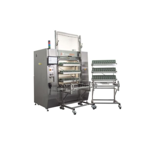
  • PBT Works – SuperSWASH

    Ideal machine for customers looking for the best cleaning results without the need for automation or very high throughput. Best solution for medium to low quantity of complex products that need to be cleaned perfectly. Application: High Density SM...

    Ideal machine for customers looking for the best cleaning results without the need for automation or very high throughput. Best solution for medium to low quantity of complex products that need to be cleaned perfectly. Application: High Density SMD Assemblies Capacity: Low to Medium Volume Contamination Solubility: Easy to Hard Handling Handling with the parts to clean is simple and safe. SuperSWASH III Reloading Stand

    PCBAs are reloaded on the dedicated reloading stand. Operators reloads frames directly into machine chamber. This minimizes downtime to zero and provides comfortable time for reload.

    Key Features

    • Ultimate cleaning performance
    • Easy operation
    • Zero drain concept
    • Linear direct spray for equal washing
    • Hot air knife direct dry
    • Illuminated glass door chamber for visual process control
    • Quick changover to Twingo – double capacity configuration
    • Wide range of standard and customized PCBA fixtures
  • PEER Group Equipment Automation Software for OEMs

    PEER Group® provides the largest portfolio of equipment connectivity and automation software products to equipment makers (OEMs) in the semiconductor and related industries. With over 100,000 licenses shipped, PEER Group is the leading supplier o...

    PEER Group® provides the largest portfolio of equipment connectivity and automation software products to equipment makers (OEMs) in the semiconductor and related industries. With over 100,000 licenses shipped, PEER Group is the leading supplier of factory automation software for Smart Manufacturing and Industry 4.0.

  • PEER Group Factory Automation Software

    PEER Group® provides the largest portfolio of factory automation software products and services to high-volume manufacturers in the semiconductor and related industries. With over 100,000 licenses shipped, PEER Group is the leading supplier of fa...

    PEER Group® provides the largest portfolio of factory automation software products and services to high-volume manufacturers in the semiconductor and related industries. With over 100,000 licenses shipped, PEER Group is the leading supplier of factory automation software for Smart Manufacturing and Industry 4.0.

  • SAKAGUCHI – Heaters

    Sakaguchi has engaged in a broad spectrum of activities encompassing heating energy created in all kinds of industries such as, electric power, petrochemical plants, electronics and environmental protection. We offer a wide range of heaters, incl...

    Sakaguchi has engaged in a broad spectrum of activities encompassing heating energy created in all kinds of industries such as, electric power, petrochemical plants, electronics and environmental protection. We offer a wide range of heaters, including heaters for flat and tubular form, liquid and gas, gas and infrared, mold heating and injection molding, compact high-output ceramic heaters and as well as other custom products.

  • Scia Systems – Ion Beam Deposition Systems – scia Coat 200 & scia Coat 500

    The scia Coat 200 is designed for homogeneous coating of 200 mm substrates, such as wafers. Typical applications of the system are multilayer films for magnetic sensors or optical coatings.

    The scia Coat 500 is designed for...

    The scia Coat 200 is designed for homogeneous coating of 200 mm substrates, such as wafers. Typical applications of the system are multilayer films for magnetic sensors or optical coatings.

    The scia Coat 500 is designed for homogeneous coating of high precision optics. Typical applications of the system are multilayer films for X-ray mirrors and filter coatings.

  • Scia Systems – Ion Beam Etching Systems – scia Mill 150 et 200

    The scia Mill 150 is designed for highly uniform Ion Beam Etching and Milling of single substrates up to 150 mm diameter. Carriers or wafers are loaded via an automatic handling system. The substrate holder has helium backside cooling and ...

    The scia Mill 150 is designed for highly uniform Ion Beam Etching and Milling of single substrates up to 150 mm diameter. Carriers or wafers are loaded via an automatic handling system. The substrate holder has helium backside cooling and can be tilted and rotated. Typical applications are the structuring of metal films for MEMS and sensors.

    The scia Mill 200 is designed for highly uniform Ion Beam Etching and Milling of wafers up to 200 mm diameter. Carriers or wafers are loaded via an automatic handling system.

  • Scia Systems – Ion Beam Trimming – scia Trim 200

    The scia Trim 200 is designed for high precision film thickness trimming in wafer processing. Typical applications of the system are frequency and thickness trimming in manufacturing of acousto-electrical devices and filters such as bulk ...

    The scia Trim 200 is designed for high precision film thickness trimming in wafer processing. Typical applications of the system are frequency and thickness trimming in manufacturing of acousto-electrical devices and filters such as bulk acoustic wave (BAW) or surface acoustic wave (SAW) devices, localized pole trimming for thin film heads (TFH) and trimming of precision thin film resistors.

    The scia Trim 200 is a high volume production system and accommodates a standard semiconductor cassette handling robot. Cluster tools with two process chambers and two cassette load-locks are available.

  • Scia Systems – Magnetron Sputtering Systems – scia Magna 200 and scia Multi 680

    The scia Magna 200 uses a unique Double Ring Magnetron architecture to achieve very high homogeneity of coatings at impressively high deposition rates. Typical applications include piezoelectric layers, optical coatings and passivation la...

    The scia Magna 200 uses a unique Double Ring Magnetron architecture to achieve very high homogeneity of coatings at impressively high deposition rates. Typical applications include piezoelectric layers, optical coatings and passivation layers.  

    The scia Multi 680 is designed for periodic multilayer coatings for substrates up to 650 mm dia. and 50 kg. Typical applications are gradient multilayer coatings of mirrors for soft X‑ray and anti-reflective coatings in UV and X‑ray applications.

  • Scia Systems – PEVCD/RIE Systems – scia Batch 350

    The scia Batch 350 is designed for homogeneous coating of several 3‑dimensional shaped substrates in one batch. Typical applications are biocompatible films for medical objects.  

    The scia Batch 350 uses a RF parallel p...

    The scia Batch 350 is designed for homogeneous coating of several 3‑dimensional shaped substrates in one batch. Typical applications are biocompatible films for medical objects.  

    The scia Batch 350 uses a RF parallel plate arrangement with rotation of each substrate for a homogeneous coating of all sides. The system is also available with an additional DC bias applied to the substrate holder.

  • Scia Systems – PEVCD/RIE Systems – scia Cube 300/750

    The scia Cube 300/750 are designed for large area high density plasma processes of substrates up to 300 mm x 200 mm (scia Coat 300) and up to 750 mm x 750 mm (scia Coat 750). Typical applications are deposition of Diamond Like Carbon (DLC...

    The scia Cube 300/750 are designed for large area high density plasma processes of substrates up to 300 mm x 200 mm (scia Coat 300) and up to 750 mm x 750 mm (scia Coat 750). Typical applications are deposition of Diamond Like Carbon (DLC) for optical filters and dielectric films for anti-reflective coatings as well as etching processes with oxygen or halogen chemistry for the structuring of Semiconductors and metals.


    The scia Cube 300/750 combine plasma excitation by an array of microwave sources. The substrate stage is equipped with an independent a RF bias. Various substrate sizes can be transferred with an automatic vacuum load-lock system.

  • SEO – Phoenix (Portable)

    The Phoenix series is designed to offer the flexibility required for QA. R&D and engineering process development. The Phoenix is a quite simple and virtually any measure size without sample cutting sample cutting preparation...

    The Phoenix series is designed to offer the flexibility required for QA. R&D and engineering process development. The Phoenix is a quite simple and virtually any measure size without sample cutting sample cutting preparation. Light-weight means simple control device and simple handling. Phoenix adopted USB type camera. Easily connect to laptop and desktop computer with Surfaceware software.

    Key Features

    • Software working on Windows 7/8/10 32bit
    • Preview function for rapidly capture image
    • Contact angle measurement range: 3- 180°
    • No required cutting sample
    • Data export to Microsoft Excel
    • Available to connect to notebook or desktop PC via USB port
    • Analysis of plasma treatment to increase the wettability of polymers surfaces
    • Adsorption / Wettability of powder and pharmaceutical products
  • SEO – Phoenix MT

    Phoenix MT is the world’s first model that can be used by turning the equipment, the individual modules can be separated, and the length of each main frame can be selected to change the model to suit almost all samples.

    Phoenix MT is the world’s first model that can be used by turning the equipment, the individual modules can be separated, and the length of each main frame can be selected to change the model to suit almost all samples.

    Key Features

    • Total flexibility: Easy to upgrade ( Manual → Auto One Drop → Multi syringes ) by modular design main frame
    • Automation : Automatic measurement progress at once
    • User friendly : Easy to transform for changed sample types
    • Tool Free changeover: Additional tools are not required for modular change
    • Changeable module position : According to sample nature, module can be change to cater for diverse sample nature/ form factor
    • Data output : Data can be exported as Excel file, offering the highest flexibility for further data processing
  • SET – ACCµRA M

    The ACCµRA M is a manual flip-chip bonder that allows ± 3 µm accuracy. This equipment permits to align manually the components with a high level of precision. The motorized arm controls precisely the bonding force. Combining and synchronizing the arm with the temperature controller, it guarantees a perfect quality and high repeatability of your process. The ACCµRA M, more than a pick-and-place system, offers thermocompression and reflow capabilities. It is the perfect equipment for universities and R&D institutes.


  • SET – ACCµRA OPTO

    The ACCµRA OPTO is a flip-chip bonder that allows ± 0.5 µm accuracy. It is dedicated to low force and reflow processes. The ACCµRA OPTO combines high precision, flexibility and accessibility. It is the perfect equipment for optoelectronics an...

    The ACCµRA OPTO is a flip-chip bonder that allows ± 0.5 µm accuracy. It is dedicated to low force and reflow processes. The ACCµRA OPTO combines high precision, flexibility and accessibility. It is the perfect equipment for optoelectronics and silicon photonics applications.

  • SET – ACCµRA Plus

    ACCµRA Plus is a flip-chip bonder designed for ± 0.5 µm accuracy in full automatic mode. It is suitable for reflow and thermocompression processes.

    ACCµRA Plus combines high pr...

    ACCµRA Plus is a flip-chip bonder designed for ± 0.5 µm accuracy in full automatic mode. It is suitable for reflow and thermocompression processes.

    ACCµRA Plus combines high precision, flexibility and short cycle time. It is dedicated to production for Optoelectronic and Silicon photonics applications.

    Applications

    • Laser diode, laser bar
    • VCSEL, photo diode
    • LED
    • Prisms, lenses, mirrors
    • Micro Assembly
    • Flip-chip bonding, die bonding
    • Chip-to-chip, chip-to-substrate bonding

    Industries

    • Optoelectronics and Silicon Photonics
  • SET – ACCµRA100

    The ACCµRA100 is a flip-chip bonder that allows ± 0.5 µm accuracy. Motorized axes guarantee a high repeatability of your process. Its flexibility makes it ideal for developing a wide range of applications. ACCµRA100 combines...

    The ACCµRA100 is a flip-chip bonder that allows ± 0.5 µm accuracy. Motorized axes guarantee a high repeatability of your process. Its flexibility makes it ideal for developing a wide range of applications. ACCµRA100 combines high precision, accessibility and cost-effectiveness. It is the perfect equipment for universities and R&D institutes.

    Applications

    • Micro assembly
    • Laser diode, laser bar
    • VCSEL, photo diode
    • LED
    • Flip-chip bonding, die bonding
    • Chip-to-chip, chip-to-substrate bonding
    • MOEMS, MEMS, MCM packaging…
    • 3D packaging
    • Nanoimprinting (UV NIL and Hot Embossing)

    Industries

    • Semiconductors
    • Memory
    • Optoelectronics and Silicon Photonics
    • Micro LEDs Displays
    • Quantum Computing
  • SET – FC150

    The FC150 is an accurate and very flexible flip-chip bonder for Chip-to-Chip (up to 100 mm) and Chip-to-Wafer (up to 200 mm) applications on the same open platform.

    The versatile design and the possibility to combine different processes make the FC150 ideal for developing a wide range of assembly applications including focal plane arrays and optoelectronic devices.

    Perfect for advanced R&D, the FC150 is also appreciated for pilot production thanks to its full automatization.


  • SET – FC300

    The FC300 is a high accuracy and high force flip-chip bonder for Chip-to-Chip (up to 100 mm) and Chip-to-Wafer (up to 300 mm) applications. FC300 covers a large range of bonding forces, from 1 to 4000N. That makes it perfectly suitable for reflow and thermocompression processes.

    The leveling between both components is adjusted before each bonding within 1 µradian. The parallelism adjustment, the high resolution alignment and the perfect control of all bonding parameters allow to achieve submicronic post-bond accuracy.


  • SET – LDP150

    The LDP150 is an electrical Press especially designed for bonding large light or radiation detectors (50 ~ 150mm). It uses compression process at room temperature (thermo-compression option available).

    ...

    The LDP150 is an electrical Press especially designed for bonding large light or radiation detectors (50 ~ 150mm). It uses compression process at room temperature (thermo-compression option available).

    A predefined gap can be achieved between two components previously pre-bonded using a high accuracy device bonder such as the SET FC150. The devices are pressed together at room temperature while preserving the initial high accuracy alignment and parallelism.

    The LDP150 is able to apply pressure up to 100,000N.

    Applications

    • Large infrared focal plane arrays
    • Military and space applications
    • Large XY, UV detector
  • SET – NEO HB

    NEO HB is a flip-chip bonder designed for ± 1 µm @ 3σ accuracy in stand-alone or full automatic mode (EFEM). It is suitable for Hybrid/Direct bonding processes. NEO HB combines high precision, flexibility and short cycle time...

    NEO HB is a flip-chip bonder designed for ± 1 µm @ 3σ accuracy in stand-alone or full automatic mode (EFEM). It is suitable for Hybrid/Direct bonding processes. NEO HB combines high precision, flexibility and short cycle time. It is dedicated for production.

    Applications

    • Hybrid / Direct bonding (room temperature)
    • Flip-chip bonding, die bonding
    • Chip-to-wafer, wafer level applications
    • Chip-to-substrate bonding
    • Pick & Place
    • Memory stacking
    • 3D IC
  • SET – NPS300

    Optimized for the production of nanostructures, the Nano imPrinting stepper Stepper NPS300 is the first ever tool able to combine Hot Embossing and UV-NIL on a same platform. The NPS300 is able to print sub-20 nm geometries with an overlay accuracy of 250 nm, when in-situ alignment is performed. Its flexible architecture offers an excellent process reproducibility and a unique ability to pattern large areas, in a sequential step and repeat mode on wafers up to 300 mm. It enables the low cost manufacturing of large stamps featuring repeated patterns.


  • SMT – Full Convection Reflow Soldering Systems

    The reflow soldering systems from SMT Wertheim stand for maximum efficiency and high product throughput with stable soldering quality. The parameterization of air flow with continuously adjustable fan units and a uniquely innovative heating zone c...

    The reflow soldering systems from SMT Wertheim stand for maximum efficiency and high product throughput with stable soldering quality. The parameterization of air flow with continuously adjustable fan units and a uniquely innovative heating zone concept enable a process-optimized soldering profile that can be flexibly applied to different products with constant temperature settings.

  • Solarius – AOP

    The AOP platform is the most flexible and modular Solarius solution for all kinds of customized measurement tasks. Depending on the indivisual task, it can be equipped with different 3D measuring sensors out the entire available...

    The AOP platform is the most flexible and modular Solarius solution for all kinds of customized measurement tasks. Depending on the indivisual task, it can be equipped with different 3D measuring sensors out the entire available technology portfolio, many sizes of motion systems and customized software. Its flexibility supports a wide variety of applications and working environments and can be tailored to meet each customer’s requirements.

    Sensor Types

    • Chromatic confocal point sensors
    • Chromatic confocal line sensors
    • Confocal matrix sensors
    • Interferometric matrix sensors
    • Focus variation matrix sensors
    • Point triangulation sensors
    • Line triangulation sensors

    The modular AOP platform can be equipped with all availabe non-destructive measurement technologies, including chromatic confocal point and line sensors, confocal area sensors, laser line triangulation sensors, interferometric sensors, and 2D camera systems. Height resolutions down to the single nm are supported same as high speed measurements of up to 80,000 points in 130 milliseconds. Vibration isolation and a lateral measurement range up to 500 mm or more make the AOP the best solution for all kinds of measurement tasks.

  • Solarius – Atlas

    The new Polaris Desktop 3D surface measuring system from Solarius enables highly accurate and precise 3D imaging of surfaces. While th...

    The new Polaris Desktop 3D surface measuring system from Solarius enables highly accurate and precise 3D imaging of surfaces. While the Polaris and the Polaris Plus are equal in accuracy and precision, the Polaris offers a cost effective variant for many applications. The Polaris Plus expands the scope of application due to its extensive equipment, which supports in particular simple automation of the measurement tasks.

    Key Features

    • Highest optical and digital resolution
    • Diffraction limited imaging
    • Reliable technology
    • ISO compliant roughness values
    • Non-contact measurements
    • Maintenance-free and robust

    Sensor Types

    • Confocal area sensors
    • Interferometric area sensors

    The Solarius Polaris 3D measuring system is based on the spinning disc confocal technique, proven over many years. In the design and calculation of the optics, great importance was attached to a physically optimal diffraction limitation ofthe optical system, which allows for accurate, precise and repeatable lateral measurements even in structural areas far below one micrometer.

    Â