Showing all 4 results

  • NTK Ceratec – Chuck repair service (6”, 8” and 12”)

    The chuck repair service is dedicated to wafer chucks damaged in device manufacturing processes to a state equivalent to new using our vast knowledge of ceramics.

    • for photolithography on ASML, Nikon, Canon, …

    The chuck repair service is dedicated to wafer chucks damaged in device manufacturing processes to a state equivalent to new using our vast knowledge of ceramics.

    • for photolithography on ASML, Nikon, Canon, …

    • for Etching/CVD on Novellus (LAM), SPTS, Anelva, Nissim, …

    Please, consult us for machine compatibilities and designs.

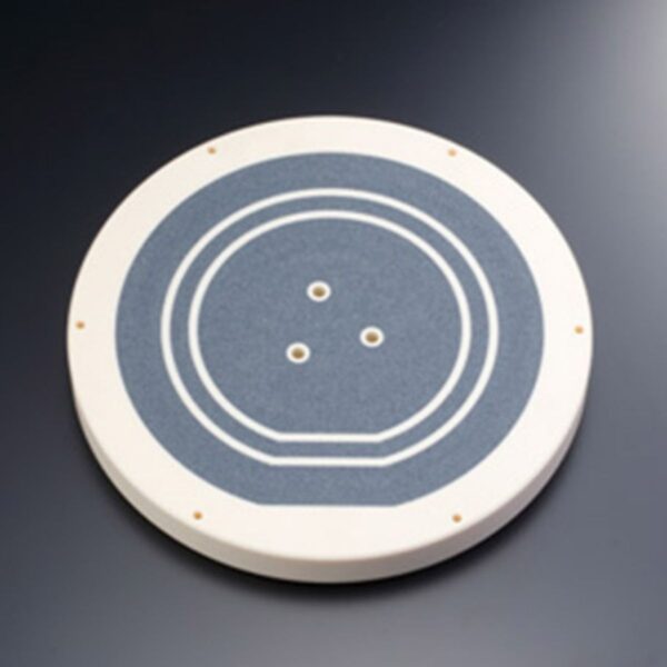
  • NTK Ceratec – Electrostatic Chuck

    Electrostatic chucks and ceramic heaters can be produced by sintering materials with metallic electrodes arranged in the ceramics. We can provide electrostatic chucks and ceramic heaters catering to user needs by utilizing sever...

    Electrostatic chucks and ceramic heaters can be produced by sintering materials with metallic electrodes arranged in the ceramics. We can provide electrostatic chucks and ceramic heaters catering to user needs by utilizing several material technologies. We can also provide services for the development and experimental production of electrostatic chucks and ceramic heaters according to region of use such as plasma and electron beam environments:

    Electrostatic chuck with heater (ESC/Heater)

    Material: AIN (Aluminum nitride)

    Electrostatic chucks (ESC)

    Material: Al2O3(Alumina) plate

    Material: Thermal sprayed Al2O3

    Ceramic heater

    Material: AIN (Aluminum nitride)

  • NTK Ceratec – Porous Chuck

    The original manufacturing method enhances adhesiveness between porous sections and base sections to achieve sufficient flatness even at boundary sections.

    We can provide highly productive and reliable wafer thinning processing and manufact...

    The original manufacturing method enhances adhesiveness between porous sections and base sections to achieve sufficient flatness even at boundary sections.

    We can provide highly productive and reliable wafer thinning processing and manufacturing requiring whole surface absorption of large sized substrates.

    We offer a wide selection of porous bodies with using different materials and pore sizes to cater to user needs.

  • NTK Ceratec – Vacuum Chuck

    We can provide optimal pin chucks tailored to strict requirements through customized design using world-class flattening process technology (flatness of 0.2 μm for 12-inch chucks).

    Can flexibly be adjusted planar shapes of pin chucks with ...

    We can provide optimal pin chucks tailored to strict requirements through customized design using world-class flattening process technology (flatness of 0.2 μm for 12-inch chucks).

    Can flexibly be adjusted planar shapes of pin chucks with variable unevenness according to the shapes of wafers and customize absorption zones and pin patterns to enhance absorption responsiveness: