")


HANMI – EMI Shield Equipment
Electromagnetic interference (EMI) shielding equipment is used to deposit stainless materials and copper onto the surface of semiconductors so that the chip shields EMI interference avoiding malfunction and assuring smooth operation with other chips.
Available in :
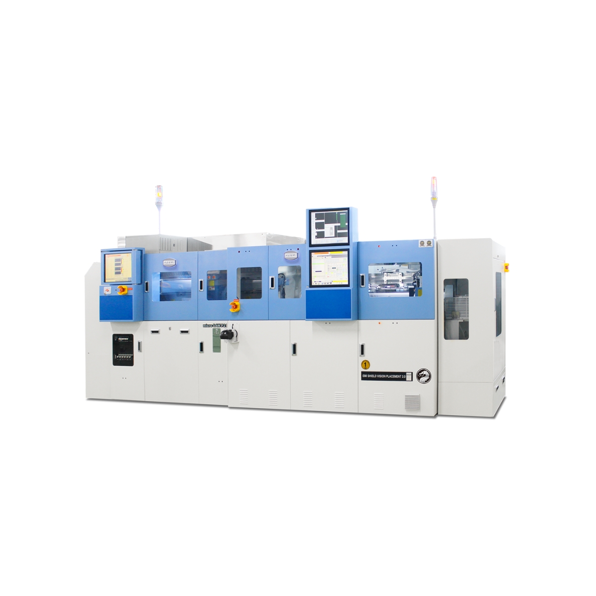
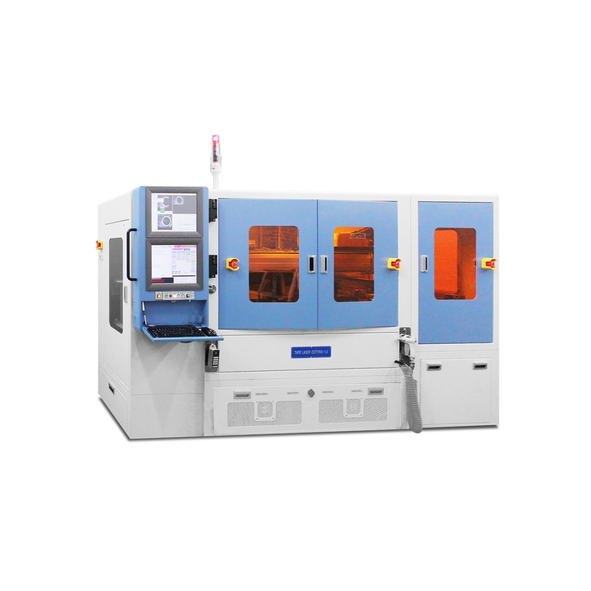
HANMI ‘s EMI Shield Equipment for the semiconductor electromagnetic wave shielding process, performs vision inspection and the very precise process of attaching semiconductor packages to jigs for sputtering. This machine offers more precise control and improved performance. If features new ‘vision auto focus’ and ‘high-speed attach mode’ which increase productivity and ease of use.
Key Features
- High productivity
- High accuracy
- Supports various brands of sputtering equipment
- Supreme vision inspection
- Small unit handling
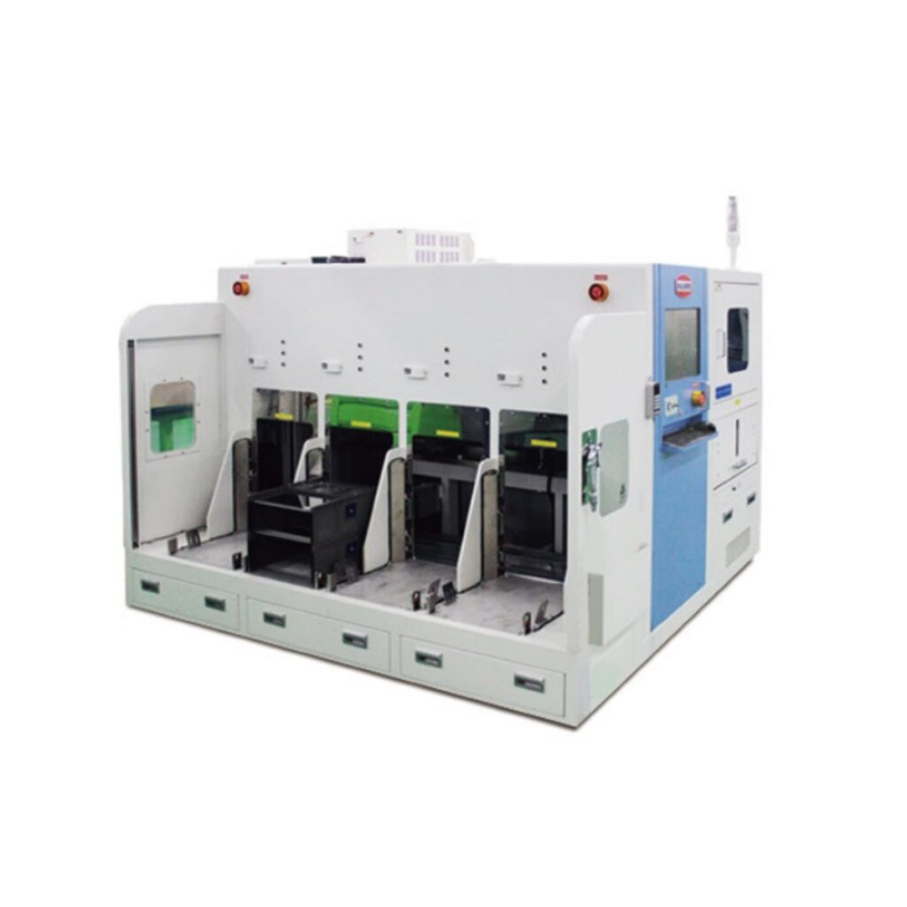
Available Models
Key Features
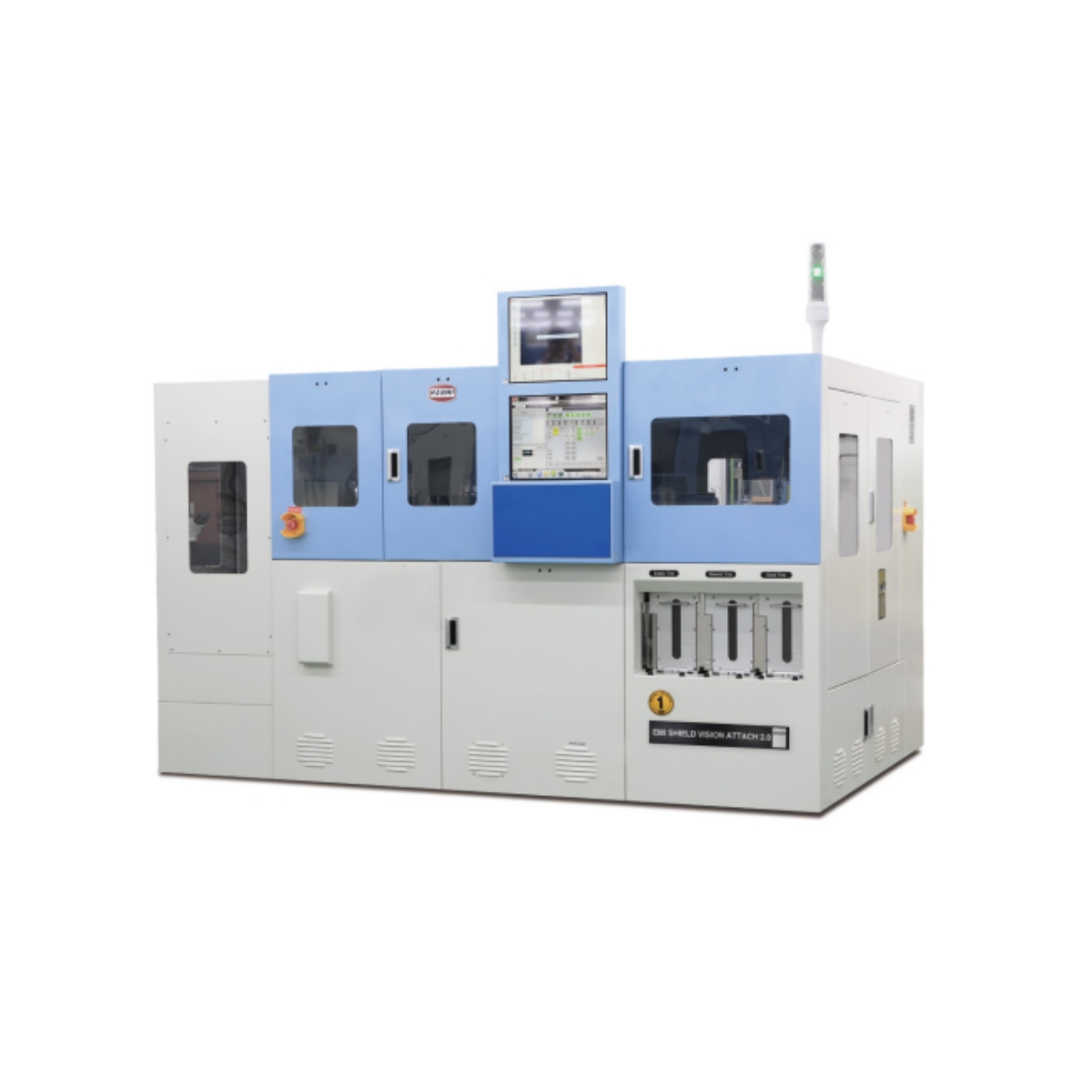
- High productivity
- Small package capability
- Supreme vision inspection
- High density substate capability
- Package traceability
- Multiple unit attach with pressure control
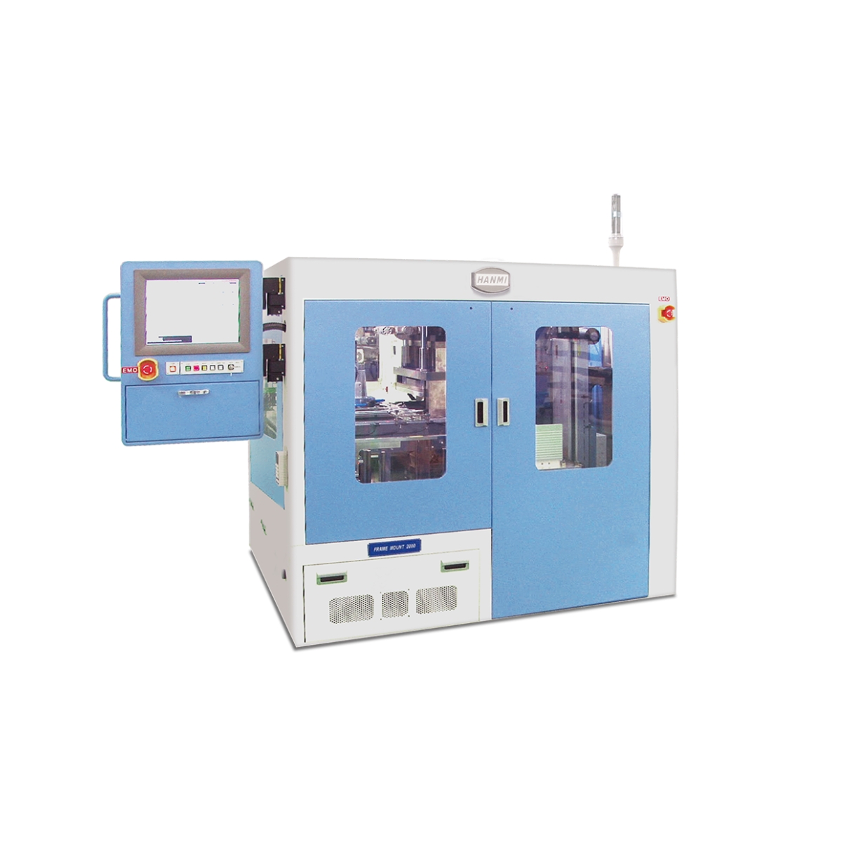
Key Features
- High productivity
- High accuracy
- Package traceability
- Bubble free with the unit pressure control
- Supreme vision inspection
- Small unit handling
Technical Specification
| Application | UPH | Sputter loading 15,000 |
| Pick & place accuracy | µm | 50µm(30µm option) |
| System performance | MTBA | 2 hours |
| MTBF | 168 hours | |
| MTTA | 3 minutes | |
| MTTR | 30 minutes |
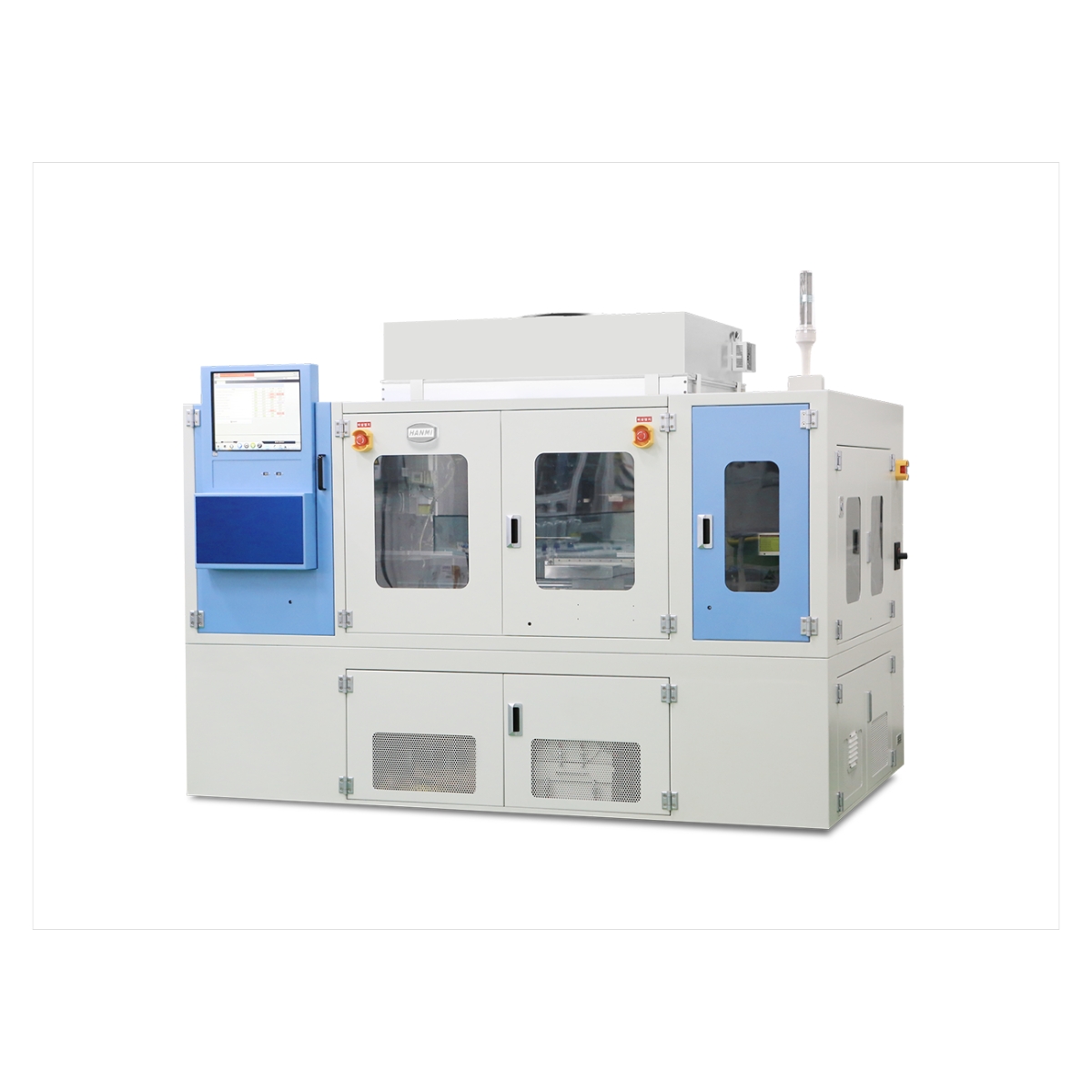
Key Features
- High productivity
- Package traceability
- Unit ejection force control
- Supreme vision inspection
- Supreme vision inspection
- Small unit handling
- Dust removal solution
Technical Specification
| Application | UPH | 15,000 |
| Pick & place accuracy | µm | 50µm(30µm option) |
| System performance | MTBA | 2 hours |
| MTBF | 168 hours | |
| MTTA | 3 minutes | |
| MTTR | 30 minutes |
Key Features
- High productivity
- Excellent taping quality
- Various material handling capability
- Bubble free attachment on frame
Key Features
- High productivity
- High accuracy
- Various handling capability
- Excellent quality
Key Features
- High productivity
- Supreme vision inspection
- Unique dust collection capability
Key Features
- High productivity
- Variety of ring type handling
- M/Z stack capability
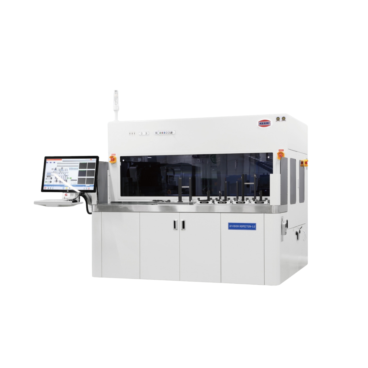
Key Features
- High productivity
- Excellent 3D vision inspection technology
- Maximum FOV 100nmx100nm


Founded in 1980 to support the development of Korea’s semiconductor industry, Hanmi Semiconductor has grown steadily into a world-class semiconductor…
